III-Sbs/Si
Integration of III-Sbs with the Si(Ge) technology
Integration of III-Sbs with the Si(Ge) technology
Staff:E. Tournié, L. Cerutti, J.-B. Rodriguez, in collaboration with A.N. Baranov and R. Teissier.
PhD students: K. Madiomanana (2011 – 2015); A. Castellano (Alcatel-Lucent, 2013 – 2016); J. Tournet (PROMIS ITN, 2015 – 2018); M. Rio Calvo (2017 – 2020); L. Monge-Bartolome (REDFINCH project, 2018 – 2021), Andres Janez Remis (LightUp project, 2020 – 2023), Michele Paparella (OPTAPHI project, 2020 – 2023).
Projects:OPTOSi(ANR blanc 2012 – 2016),MOREMIR(ANR P2N 2013 – 2016),ANTIPODE(ANR, 2014 – 2018),PROMIS(H2020 Marie Curie 2015 – 2018),REDFINCH(H2020, 2017 – 2021),OPTAPHI(H2020, 2020 – 2023),LightUp(ANR, 2020 – 2023), FILTER (Franco-German ANR, 2021 – 2024).
Other collaboration:G. Patriarche,C2N, Palaiseau (France) ; A. Trampert,Paul-Drude-Inst., Berlin (Germany) ; T. Baron,LTM, Grenoble (France) ; Kei May LAU,HKUST(Hong Kong)
Past collaboration:G. Roelkens, U.Ghent, (Belgium).
Combining the maturity of the silicon technology with the optical and electrical properties of the III-V semiconductors is under active consideration for developing novel optoelectronic devices, like photonic integrated circuits (PICs) or high-frequency transistors. The main foreseen applications are datacom, integrated sensors and multi-junction solar-cells. Long wavelengths (l > 5 µm) require to move toward Ge-rich SiGe photonic structures to avoid absorption due to Si-based materials (SiO2, SiNx, Si).
The most mature approach today to integrate III-Vs on Si is theheterogeneous integration. III-V heterostructures are first grown on their native substrates before being bonded as individual dies or as a whole wafer onto the Si platform. Still, on a longer term large scale integration of photonic circuits will more surely rely on the direct epitaxial growth of III-Vs on Si,i.e.themonolithic integrationof optoelectronic devices on silicon as put forward on the road map of all electronics majors.
In the last decade, nanoMIR has been active in the two approaches, heterogeneous and monolithic integration, with recent effort toward monolithic integration.
Regarding heterogeneous integration, we designed and grew dedicated III-Sb mid-IR lasers and photodetectors to be heterogeneously integrated on CMOS compatible platforms by G. Roelken’s group at U. Ghent/IMEC. The results have been published in several papers that can be tracked in thepublication lists(Years 2011 to 2014).
As for monolithic integration, we investigate the direct growth of III-Sb compounds on Si substrates. We started with growth on offcut Si substrates to avoid the formation of antiphase domains and boundaries (APBs), a type of defect which generates shorts in devices and which should absolutely be avoided. After demonstrating the first cw operation of mid-IR laser diodes (Reboulet al.,Appl. Phys. Lett. 99 (2011) 121113) we returned to more fundamental studies of the initial growth stages. We have first established a simple and reliableex-situSi-surface preparation prior to epitaxy, and we have performed an in-depth study of the microstructure and defect properties of GaSb/Si epitaxial layers in collaboration with C2N, CEMES, INSA-Rennes and PDI-Berlin. These results allowed optimizing the growth initiation on miscut Si substrates, and to understand the origin of most defects. The data are available in a number of papers published in Acta Materiala, Appl. Phys. Lett., J. Cryst. Growth and Phys. Rev. Mat. Elaborating on this background we have demonstrated the first ever quantum cascade lasers grown on silicon (Nguyen-Vanet al.,Sci. Rep. 8, 7206 (2018)).
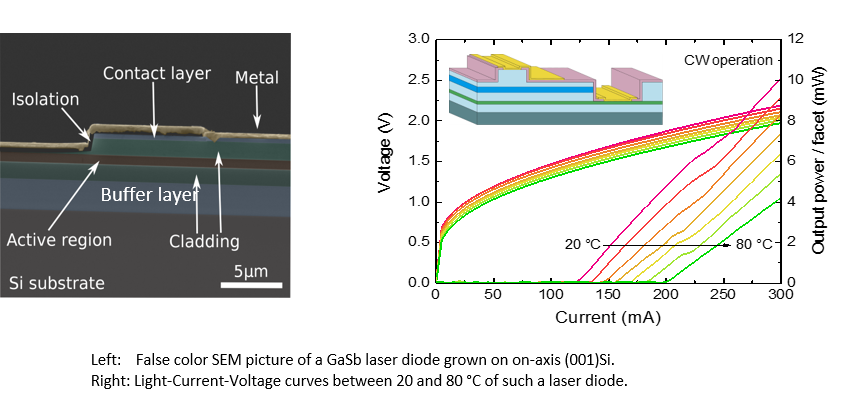
To go further, and to open wider possibilities in terms of applications, we are currently working toward the epitaxial integration of these devices on on-axis Si substrates. On one hand we collaborate with several groups providing on-axis MOVPE III-V-on-Si templates. Lasers diodes have been demonstrated on GaSb-on-Si and GaAs-on-Si templates. On the other hand, we have implemented in-house a new strategy for the III-V-on-Si nucleation stage. This strategy promotes the annihilation of APBs within the first ~500 nm GaSb buffer layer. Mid-IR laser diodes (Rio Calvoet al.,Optica 7(4), 263 – 266 (2020)) as well as quantum cascade lasers (Loghmariet al.,APL Photonics 5, 041302 (2020)) grown on on-axis (001)Si could be demonstrated. OSA launched apress releaseon these results.
Next, we will be focusing on one hand on reducing the threading defect density in the structures and on the other hand on integrating the optoelectronics devices with photonics integrated circuits rather than on bare Si substrates. We have already developed an etched-facet diode technology for this purpose (Monge Bartolomeet al.,Optics Express 28 (14) 20785 (2020)).
In addition, in 2020 we started working on integrating optoelectronic devices on SiGe-based platforms for long-wavelength applications.