WELCOME TO NANOMIR

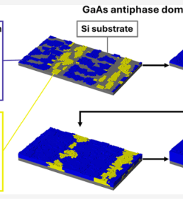
NanoMIR is a world leader in III-Sb technology,i.e.the family of III-V compounds based on GaSb, InAs, AlSb, InSb, their alloys and their heterostructures. It aims at developing this technology and its applications.

The antimonides (III-Sbs) are III-V semiconductors with effective band gaps particularly well suited to the mid-infrared (mid-IR ~ 2–12 µm), a wavelength range which exhibits transparence windows of the atmosphere as well as strong absorption lines from many gas species. The mid-IR is thus very well suited to develop a variety of applications with important societal impact such as gas analysis (pollution or process monitoring, physics of gases, of the atmosphere,…), medical applications (surgery, diagnosis,..), free-space communications, but also security- and defense-related applications (counter measures, detection of toxic or explosive species, night vision,…).
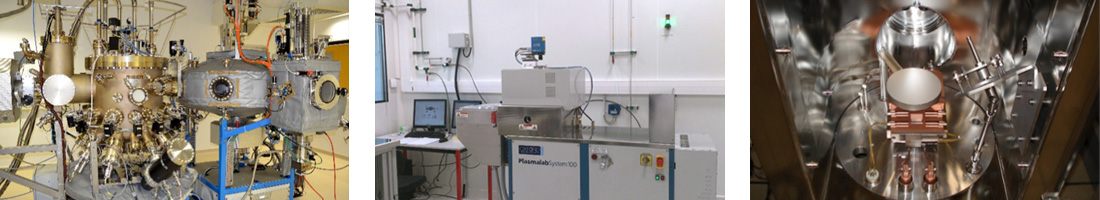
For the last ten years, nanoMIR has been mainly focusing on developing mid-IR optoelectronic devices (lasers, photodetectors, highly-coherent laser sources) for these applications. It has achieved a number of breakthroughs which can be traced back in the list of publications.

Another objective of the group is to perform more fundamental studies and to explore the full potential of the III-Sb technology. So, activities on the integration of the III-Sb devices with the Si technology, on all-semiconductor plasmonics or on gas sensors have recently appeared. On the other hand, new exploratory topics (Optical Parametric Oscillations, topological insulators, concentrated photovoltaics,…) are emerging.

RESEARCH TOPICS

Here you have a brief description of nanoMIR’s research topics. You can find more about each of these topics in their dedicated pages.

The nanoMIR group develops a number of III-Sb-based lasers: GaInAsSb/AlGaAsSb quantum well laser diodes, GaInSb/InAs interband cascade lasers and InAs/AlSb quantum cascade lasers. Combining these three systems allows covering the whole wavelength range from 1.5 µm to 25 µm. GaAs-based QCLs are investigated for THz emission. Mid-IR DFB and VCSELs deliver the single frequency emission needed for gas analysis.

READ MORE >

Quantum detectors based on Ga-free InAs/InAsSb type-2 superlattice (T2SL) and Ga-containing InAs/GaSb T2SL in XBn and XBp barrier structure designs are fabricated and studied for high performance IR imaging.

READ MORE >

The mid-IR wavelength range exhibits transparence windows of the atmosphere and fingerprint absorption lines of a number of interesting – whether positively or negatively – gases. It is the best wavelength range to develop sensing systems based on tunable absorption spectroscopy. The nanoMIR group works on such systems, focusing lately on quartz-enhanced photo-acoustic spectroscopy.

READ MORE >

Highly doped semiconductors based on III-Sbs are used to overcome the limitations of gold and silver as traditional materials in the field. The main topics developed are biosensing integrated in microfluidic circuits, thermal emission with complex metamaterial heterostructures and gap-plasmon structures for mid-IR applications.

READ MORE >

Integrating III-V semiconductors and devices with the Si technology offers the promise to benefit from the best of both technologies. The nanoMIR group investigates the epitaxial integration of III-Sb-based optoelectronic devices on Si substrates, where the devices are directly grown on Si. It has also an action in the heterogeneous integration, where devices are bonded on the Si substrate or PIC.

READ MORE >

The objective of the nanoMIR is also to develop new applications of the III-Sb technology. For example, upstream work has been recently carried-out on GaSb-based non-linear heterostructures, on topological insulator phases, on Novel diagnostic tools for nano-characterization of photonic devices, or on whispering gallery mode lasers, to name but a few.

READ MORE >

NanoMIR competences span the whole field from semiconductor-nanostructure epitaxy to device and system-prototype implementation, via heterostructure characterizations, design, processing and investigations of devices. To reach our objectives, the group has a number of fabrication and characterization set-ups devoted to material and device studies. In particular, we run three molecular-beam epitaxy (MBE) systems, several FTIR spectrometers and clean room equipment for processing technologies.

NanoMIR is a research group of “Institut d’Electronique et des Systèmes”, a research laboratory ofUniversité de Montpellierjointly operated by CNRS (UMR 5214). The research is carried on by 13 permanent scientists and, typically, 5 to 10 PhDs students or post-docs.

Four technical  staff (J.M. Aniel, G. Boissier, A. Meguekam, G. Narcy) actively and efficiently support the research efforts.

NanoMIR is or has been supported by a number of institutions such as the European Union (FP6, FP7, H2020 programs), the French “Agence Nationale de la Recherche”, the French “Délégation Générale de l’Armement”, theRégion Languedoc-Roussillon, ADEME, SaTT AxLR…

NanoMIR has been awarded anEquipEx(project “EXTRA”) by the French program on “Investments for the Future” and it is a founder of the international CNRS laboratoryILNACS.

LAST NEWS

News