IR Quantum Detectors
Staff: P. Christol, J.-P. Perez
PhD students: M. Bouschet (Cifre-LYNRED, 2019-2023) ; C. Bataillon (ADS-Région Occitanie, 2020-2023) ; M. Tornay (Cifre-Défense AID-LYNRED 2022-2025) ; H. Mezouar (I2S-Région Occitanie, 2023-2026).
Projects: HOT-MWIR (ANR C24 2018-2022), CNES (R&T CNES 2019-2023), ONERA (ONERA contract 2019-2022), AIRBUS-DS (2020-2023), LYNRED (2019-2023), LYNRED-2 (2022-2025)
Main collaborations: I. Ribet (ONERA-Palaiseau), N. Péré Laperne (Lynred), O. Gilard (CNES), O. Saint-Pé (ADS).
Objective
The main objective is the fabrication and the study of high performance cooled infrared (IR) quantum detectors made of Ga-free InAs/InAsSb type II superlattices (T2SL) in barrier architectures (XBn structures). These Sb-based photodetectors should be able to improve the signal to noise ratio to satisfy the criteria of SWAP (Size, Weight and Power) requirements with high operating temperature (T > 150K) in the Midwave IR (MWIR 3-5µm) to address specific military and spatial applications.
Recent results
1. Ga-free T2SL detectors for high temperature operation
To achieve operation at T=150K with the highest performance and address the MWIR broadband (lamba cut-off = 5µm), XBn InAs/InAsSb Ga-free T2SL have been grown by MBE on GaSb substrate. In the framework of the ANR project HOT-MWIR, involving IES, LPENS, ILV, 3-5 Lab, ONERA and Lynred, dark current density as low as 2×10⁻⁶ A/cm2 at 150K (Vbias = -400mV) and quantum efficiency (QE) higher than 50% (Fig. 1a) have been reported. Such results demonstrate the potentiality of the Ga-free IR detector technology and show that carriers transport is not as anisotropic as previously thought. To improve performance of the device, understanding anisotropic behavior is under investigation. In particular, recent transmission electron microscopy (TEM) measurements, performed by C2N, highlight a strong segregation of antimony (Sb) at the T2SL interfaces, thus disrupting the schematic representation of abrupt bidimensional quantum potentials (Fig. 1b), without nevertheless altering the optical properties.
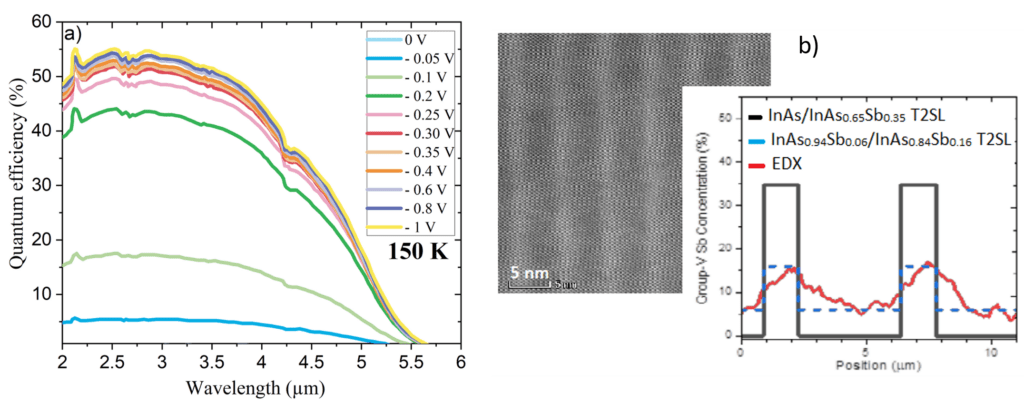
Fig. 1: InAs/InAsSb T2SL XBn detector a) Front side illuminated spectral quantum efficiency performed at 150 K for different applied voltage ; b) Cross-sectional high-resolution TEM images showing antimony concentration (Sb) in the T2SL period : experimental EDX linescan (red curve) ; nominal Sb concentration profile (black solid line) ; average Sb concentration from EDX scan (blue dashed line).
Additionally, the first Ga-free T2SL focal plane array (FPA) in VGA format (15µm pitch) has been fabricated (Fig.2a). Such a hybridized device displays IR images with operability equal to 99.6% and a Modulation Transfert Function of 0.47 at Nyquist frequency (Fig. 2b).
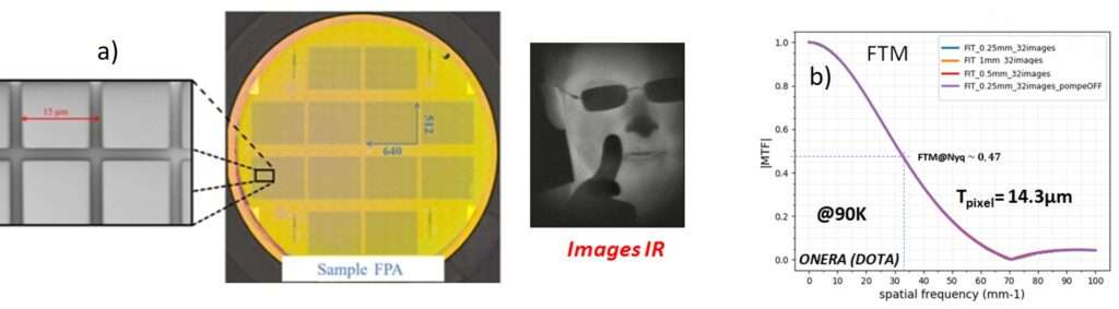
Fig. 2: InAs/InAsSb T2SL detector FPA : a) FPA in VGA format with 15µm pitch with associated IR images recorded at 130K ; b) Modulation Transfer Function of the red MWIR VGA 15µm FPA recorded at 90K.
More details can be found in Bouschet et al. and Bouschet et al..
2. Ga-free T2SL detectors under proton irradiation
In the context of the R&T CNES project, 60 MeV proton irradiation with fluence up to 8×10¹¹ H+/cm² was applied to Ga-free InAs/InAsSb T2SL XBn barrier detector having different absorbing layer thickness (AL). For device maintained at its targeted operating temperature (150 K) for which the current is dominated by diffusion process, a degradation of dark current of only a factor 2 and reduction of the R0A product value are observed under proton irradiation due to displacement damage dose effects (Fig. 3) and the XBn behavior of the device seems to disappear. Additionally, we observe a decrease in minority carrier lifetime as a function of the barrier layer (BL) thickness and implications on QE remain to be evaluated.
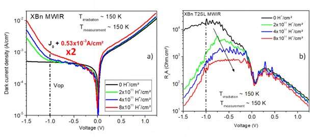
Fig. 3: InAs/InAsSb T2SL detector under proton irradiation : Dark current density-voltage (J-V) characteristics (a) and R0A product (b) measured at 150 K before irradiation (in black) and after proton irradiation of 8×1011 cm-2.
Thanks to TCAD simulations, we identify the different dark current regimes after irradiation. At reverse voltage, the device is dominated by Fowler-Nordheim (FN) at the BL/AL interface while generation-recombination (G-R) and trap assisted tunneling (TAT) currents are revealed in the AL. However, more investigations at lower fluence are planned to understand these phenomena and then to purpose new T2SL detector design or process to overcome proton irradiation. More details can be found in Bataillon et al..