RESEARCH
NanoMIR’s competencies cover the whole range from semiconductor nanostructure epitaxy to device and system prototype implementation, heterostructure characterization, design, processing and device studies. To achieve its goals, the group has a number of fabrication and characterization facilities dedicated to materials and device studies. In particular, we operate three molecular beam epitaxy (MBE) systems, several FTIR spectrometers, and clean room equipment for processing technologies.
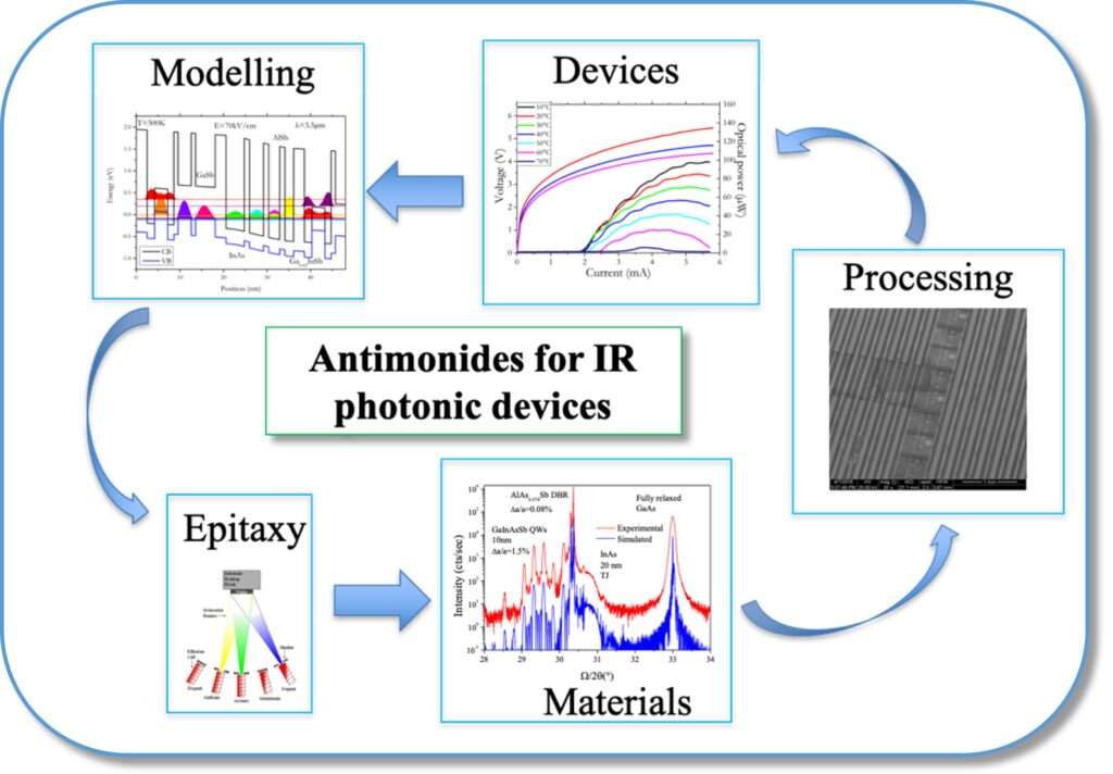
During the last couple of decades, nanoMIR has mainly focused on the development of mid-IR optoelectronic devices (lasers, photodetectors) for these applications. It has achieved a number of breakthroughs which can be seen in the list of publications.
The goal of nanoMIR is also to develop new applications of the III-Sb technology. For example, upstream work has recently been done on GaSb-based nonlinear heterostructures, on topological insulator phases, on free-space optical communications, or frequency combs on single-section laser, to name a few.