III-V on Silicon
Staff: L. Cerutti, J.-B. Rodriguez, E. Tournié.
PhD students: M. Rio-Calvo (2017-2020), L. Monge-Bartolome (2018-2021), M. Paparella (2020-2023), A. Remis (2020-2023), A. Gilbert (2021-2024), M. Silvestre (2023-2026), S. Lacaze (2024-2027), S. Boulos (2024-2027).
Projects: REDFINCH (EU, 2017-2021), OPTAPHI (EU, 2020-2024), UNISON (EU, 2024-2028), PHC PROCOPE, ANR PIANIST, ANR NUAGES, ANR-DFG FILTER, ANR LIGHT-UP, ANR-DFG LICORICE.
Objective
Our work focuses mainly on the growth of antimonide-based materials and devices on Silicon substrates. Key challenges include the substrate preparation, the study of the nucleation step and the design of the buffer layer in order to i) prevent the formation of micro-twins and cracks, ii) achieve an early burying of the antiphase domains and iii) decrease as much as possible the threading dislocation density. III-Sb/Si templates are then used to realize IR lasers which paves the way for their monolithic integration with photonics integrated circuits.
Recent results
1. Antiphase domains burying
We have clarified the mechanism and conditions that enables the burying of the antiphase domains. We have experimentally demonstrated that the initial spatial distribution of the two phases could be random or perfectly organized in the form of alternating stripes following the terrace geometry at the Si surface (Fig. 1). Our study demonstrate how in both cases, the substrate residual miscut and the natural anisotropic growth of the III-V can be used to favor the growth of one domain which in the end leads to the burying of the slowest. This approach has been extended to other III-Vs (InAs, GaAs) and an other group IV substrate (Ge), which validates the burying model. More details can be found in Rio-Calvo et al., Gilbert et al., and Gilbert et al. Collaboration : FOTON, C2N.
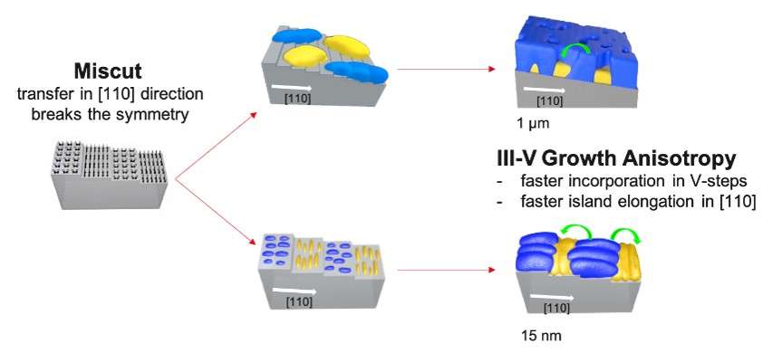
Fig. 1: Scheme of antiphase domain burying. Left panel: the silicon surface exhibits dimers rotated by 90° on adjacent terraces. Top panel: large initial III-V islands nucleate randomly and extend over several terraces while keeping the same polarity. Under step flow growth conditions, the fastest growing domain overgrows the slowest one. This configuration is typical for GaSb growth on Si. Bottom panel: small islands nucleate on the terraces, which governs their polarity. The growth anisotropy results in one domain burying the other one. This configuration is typical for GaAs growth on Si.
2. Reduction of the threading dislocation density for GaSb grown on Si
The density of threading dislocations generated during the growth of III-Sb on Si is huge and is related to the relaxation of the strain introduced by the 12% lattice parameter mismatch. We studied the reduction of the density by inserting a relatively thick AlSb layer into the GaSb buffer. The strain introduced by this layer promotes the gliding of the threading dislocations, and therefore enhances their interaction and annihilation. A thorough study of this relaxation process as well as an optimization of the different parameters allowed us to reach a record low density of 1.7×107 cm-2 obtained for a total buffer thickness of 2 µm (Fig. 2). More details can be found in Gilbert et al.. Collaboration : PDI.
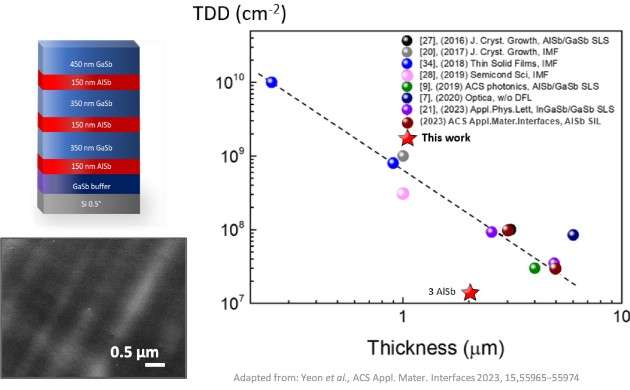
Fig. 2: Top left: Sample structure. Bottom left: ECCI of a sample. An emerging dislocation appears as a bright spot on the image. Right: Evolution of the threading dislocation density with the sample thickness, for various approaches found in the litterature.
Other investigations are underway to break this record and further reduce the threading dislocation density.
3. Photonic integrated circuits (PICs)
Diode lasers have been for the first time monolithically integrated with SiN waveguides (Fig. 3). The waveguide structure was first deposited, and a recessed area was realized in order to perform the epitaxy of the III-Sb buffer layer as well as the laser heterostructure. A specific technological process was then developed to remove the amorphous material, and to form the optical cavity facets through etching. This optical coupling opens the way to the laser integration with more complex integrated photonic chips for sensing applications for example. More information can be found in Monge-Bartolome et al., Paparella et al., Remis et al., and Paparella et al. Collaboration: MTU, C2N, LNESS.
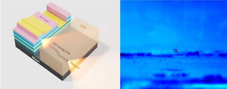
Fig. 3: Left: scheme of the PIC with a diode laser integrated with a passive SiN waveguide. Right: IR camera picture of the waveguide end. The bright spot is the light emitted by the laser, coupled into and transmitted through the SiN waveguide.
Further work will focus on integrating interband cascade lasers with SiN PICs and quantum cascade lasers with SiGe-based PICs, and on developing integrated sensors.