Plasmonics
Plasmonics
Staff:T. Taliercio, F. Gonzalez Posada, L. Cerutti, J.B. Rodriguez, E. Tournié.
Post-doctorant position:M.-J. Milla (2015-2017), F. Barho (2018-2019), P. Loren (2020-2021).
PhD students: F. Barho (2014 – 2017), F. Omeis (2014-2017), M. Bomers (ITN-PROMIS, 2015 – 2018), E. Alvear (2016-2019), C. Maës (2017-2020), M. Najem (2019-2022), P. Fehlen (2020-2023), J. Guise (2020-2023).
Projects:SUPREME-B(ANR 2014 – 2018),PROMIS(H2020 Marie Curie 2015 – 2018), SETES (SATT project 2018), SEA (pre-maturation Occitanie, 2020-2021), NanoElastir (ASTRID 2020-2023).
Other collaborations: A. Mezy, A. Garcia (Sikémia-France), G. Lerondel, A. Bruyant (Université de Technologie de Troyes-France), J. J. Greffet, J. P. Hugonin (Institut d’Optique (France), Y. De Wilde (Institut Langevin-France), E. Centeno, R. Smaali, A. Moreau (Institut Pascal-France), P. Biagioni (Politecnico di Milano), François Lagugné (London, Canada).
Plasmonics is a very important field of research of nanophotonics. In Montpellier, we decide to approach plasmonics in an original way. We propose to develop metal-free plasmonics. Indeed, heavily doped semiconductors (HDSC) can replace current metal such as gold or silver. HDSC are particularly well adapted for Mid-IR and THz plasmonics. The theme plasmonics developed in the NanoMIR group is focused on three main projects: Plasmonics for biosensing, Gap plasmons and hyperbolic metamaterials, Active plasmonics.
Why using HDSC such as Si-doped InAs instead of noble metals such Au, Ag? First of all, HDSC are CMOS-compatible, which paves the way toward their integration in low-cost, mass-fabricated devices. Secondly, the plasmonic properties of HDSC based nano-antennas subsist until the THz range while noble metals (Au, Ag) behave as a perfect conductor without plasmonic properties. Furthermore, HDSC maintains the plasmonic properties by adjusting their doping level to bring their plasma frequency in the adapted spectral range. Finally, HDSC internal losses, such as those of Si-doped InAs, are two orders of magnitude smaller than those of Au.
Plasmonics for biosensing:
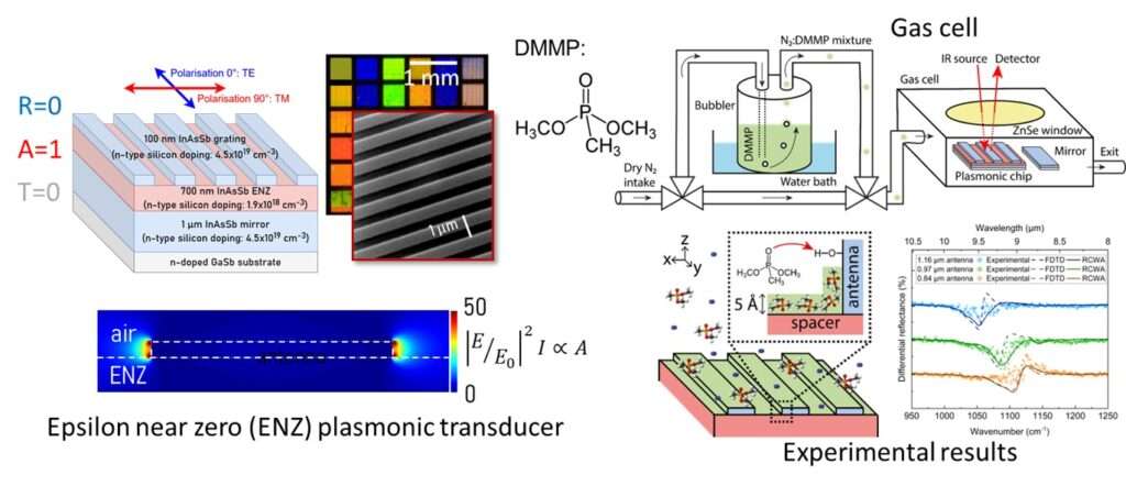
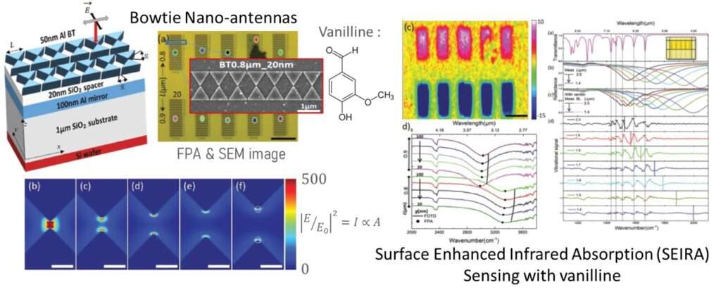
Highly doped semiconductors (HDSC) are the best candidates for Surface-Enhanced Infrared Absorption (SEIRA) and/or infrared surface plasmon resonance (SPR). Recently, we have demonstrated these potential applications theoretically and experimentally. We have generated localized SPR (LSPR) in the infrared using heavily Si-doped InAsSb layers grown lattice-matched on GaSb substrates. We have designed and fabricated an optimised HDSC-based LSPR optical transductor, to reach resonances in the 6-15 µm IR range for SEIRA or SPR measurements. Vanillin molecules have been detected with less than 12 femtograms/antenna of molecules and enhancement factor as high as 15 000. These values are the state-of-art of SEIRA experiment based on HDSC antennas (Fig. 1a). Much more recently, we have developed a new spectroscopy technique based on HDSC nano-antennas: the Surface Enhanced Thermal Emission Spectroscopy, SETES. Surface-enhanced consists of using perfect absorber metamaterial (PAM) to emit efficiently light in the mid-IR. The PAM is coupled to molecules (11-pentafluorophenoxyundecyl-trimethoxysilane, PFTMS) functionalized at its surface. The surface functionalization of the PAM by the molecules perturbes its thermal emission (Fig. 1(b)).
Fig. 1:(a) SEIRA experiments with vanillin. Thin lines are LSPR without vanillin, thick lines are LSPR with vanillin. (b) SETES experiments with a PFTMS self-assembled monolayer (SAM) (violet line) and without SAM (black line).
Gap plasmons and hyperbolicmetamaterials
Gaps plasmon are plasmonic structures able to control accurately the phase and amplitude of the reflected or the transmitted light. They consist in a small dielectric layer sandwiched between two metallic layers. They allow to imagine new optical functionalities (perfect absorber, polarization control, …). Using HDSC gives us the possibility to explore new possibilities of metamaterial or metasurface exclusively based on semiconductors. We experimentally demonstrated perfect absorption from the Mid-IR (8 µm) to the Far-IR (50 µm) and demonstrated that HDSC maintain the plasmonic properties in this wide spectral range and up to the THz (Fig. 2(a)).
Fig. 2:(a) Ribbon antenna deposited on a thin dielectric layer and a thick layer of HDSC give gap plasmon modes. Their absorbance is measured (solid lines) and simulated (dashed lines) for different ribbon width. (b) LDOS investigated by TRSTM. The HM consists in stacked layers of doped and un-doped InAs.
Hyperbolic media (HM) are also a promising topic. They consist in stacked layers of a few tens of nm alternating metal and dielectric. These stacked layers of doped and un-doped semiconductors can be considered in specific conditions such as metamaterial. The near-field optical properties of these metamaterials can be controlled by adjusting the geometry and the doping level of the layers. Thermal Radiation Scanning Tunneling Microscopy (TRSTM) allows to investigate accurately the local density of states (LDOS) and to understand the physical properties of these metamaterials (Fig. 2(b)). HM offer the possibility to access hyperbolic dispersion relation for electromagnetic waves thanks to the permittivity values along or perpendicular to the normal axis to the surface being positive or negative.
Active plasmonics
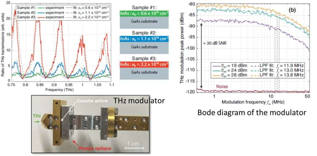
HDSC allows to develop integrated plasmonic functionalities into optoelectronic devices. Thanks to the possibility to adjust optically or electrically the carrier density into semiconductor, we can tune dynamically the plasmonic properties of the HDSC. Theoretical investigations have been done to optically tune the plasmonic properties of photo-generated metasurfaces in the THz range. We recently demonstrated the possibility to optically modulate a THz wave at a frequency of a few MHz (Fig. 3). We also designed and fabricated a guided-mode resonant (GMR) filter based on HDSC. So far, the GMR filter cannot be activated. However, this approach demonstrated the possibility to integrate the GMR filter directly on an optoelectronic device, such as, a mid-IR detector.
Fig.3: The transfer function of the InAs slab: the dots correspond to the experimental data and the solid line to their fit with a first-order low pass filter. The inset of the figure shows the THz spectrum measured using a 10 Hz resolution bandwidth for a laser amplitude modulation frequency of fm=5 kHz.
HDSCs are probably the best-suited approach to develop active plasmonic optoelectronic devices. We can imagine a few applications, such as, active filter for detector, beam shaper for THz beam, …